High Throughput Digital Lithography Development Enables AI and HPC Device Integration
The development of high throughput maskless exposure technology for 2.5D and 3D integration has been a subject of considerable R&D efforts in recent years. In this study, we employed the LITHOSCALE® XT system, a proven technology for UHD FO WLP, to digital lithography patterning of redistribution layer (RDL) and VIA structures for application in Fan-out panel level packaging (FO PLP).
The FO PLP technology signifies an expanding domain within the overarching category of FO packaging technologies. This trend is driven by the impetus experienced by designers seeking to transition from wafer-based approaches to panel configurations. This strategic shift is motivated by the objective to maximize the efficiency of the multi-die packages and to optimize the cost of ownership (CoO). The digital lithography patterns were applied to a substrate dimensions, 300×300 mm², glass and silicon respectively, by using high resolution PI dielectric material. The CD distribution is illustrated in Fig. 1.
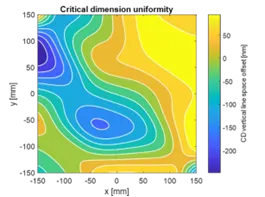
Figure 1: CDU – contour plot of the critical dimension distribution evaluated as vertical line distance in writing orientation. Sampling was performed in a l→r, t→b raster scan fashion. No vertical striping is visible in the scan direction
Recent advancements in software architecture have been optimized to address the demands of sophisticated 3D integration representing a significant technological innovation that addresses the requirements for future AI and HPC devices. The utilization of advanced software constitutes a pivotal element in the operation of the Zero Stitch feature and the dynamic "on–the–fly" compensation that is imperative in heterogeneous integration processes. For investigating the image and resist performance a range of test patterns were implemented ranging from dot arrays, straight & diagonal free-standing and parallel lines to circles and wedges as they are used in a wide range of applications. The 'Siemens Stars' are structures that are commonly avoided during real–application processing, since they challenge the exposure process literally in all directions. The central resolution breakdown circle at the 2 µm-L/S level shows that the L/S-ratio becomes biased towards the intrinsic resist behavior. The slight bridging between the sub–resolution beams at the center is caused by digital sampling of the exposure system.
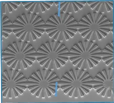
Figure 2: The 'Siemens Stars' patterns prove straight edge contour of patterns in all lateral directions. The 'Zero Stitch' is not visible over the multiple patterns
Furthermore, the system's advanced capabilities make it particularly well-suited for applications involving multi-die patterning of large die interposers, MEMS, advanced imaging, and die traceability for security and automotive purposes. The LITHOSCALE® XT fully digital platform has been demonstrated to ensure large die size patterning capabilities, with no design restrictions in 3D integration. This development is poised to establish a novel industry standard in the domain of digital patterning systems for both advanced packaging designs. Innovative equipment overcomes the limitations of legacy exposure technology, especially for large die sizes interposer patterning.
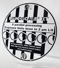
Figure 3: Glass wafer, tilted view, patterned by black resist illustrating the features of the high throughput system: six exposure heads, proving fulfilled layout, wafer edge zone exposure control feature