Domain Knowledge-Driven Fusion Machine Learning for Overlay Prediction Enhancement
Continuous device scaling in semiconductor manufacturing has pushed fabrication processes towards their phys-ical limits,1 making overlay control increasingly challenging such as critical dimension (CD), overlay, and edge placement error (EPE).2 Conventional feedback control methods struggle with rising process complexity,3 while metrology throughput constraints limit measurement sampling, hindering real-time control. Although advanced machine learning (ML) algorithms show promise for overlay control,4 traditional ML approaches lack theaccuracy required for high-volume manufacturing.5
To address these challenges, we developed a novel overlay prediction framework integrating domain-specific process knowledge with advanced machine learning. By combining multiple scanner and overlay datasets, we leveraged stochastic process variations and expert domain insights as engineered features. The data were pre-processed with semiconductor-specific techniques and fed into a fusion ML model capable of learning from heterogeneous feature types. This domain knowledge-driven approach captured complex process signatures ef-fectively. Training was augmented with large-scale synthetic data mimicking real process patterns to cover edge-case scenarios.
Our results demonstrate significant improvements in overlay prediction accuracy. Using 70% of data for training and 30% for testing, a baseline XGBoost model achieved only about R2 ≈ 0.43 with an overlay root-mean-square error (RMSE) >2 nm. In contrast, our domain-informed fusion ML model attained R2 ≈ 0.98, with RMSE <0.2 nm, representing a 2.3× improvement in R2 and a 10× reduction in RMSE. This metrology-grade accuracy enables real-time, full-field overlay predictions for inference-based control. By integrating ML-driven corrections with conventional control loops, semiconductor fabs can maintain critical layer alignment within tolerance despite limited measurements and increasing process complexity.
Keywords: Overlay, Prediction, Fusion machine learning, Inference-based control
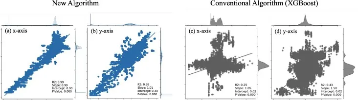
Figure 1. Model accuracy comparison both axes: proposed algorithm for (a) x-axis and (b) y-axis versus XGBoost for (c) x-axis and (d) y-axis
*E-mail: [email protected]
ACKNOWLEDGMENTS
This work was supported by the Technology development Program(RS-2025-25461995) funded by the Ministry of SMEs and Startups(MSS, Korea)
REFERENCES
- Bohr, M., “A 30 year retrospective on dennard’s mosfet scaling paper,” IEEE Solid-State Circuits Society Newsletter 12(1), 11–13 (2007).
- Jee, T., You, J., Lee, H.-G., Hong, S., Cho, J., Lee, T., hyun Seo, J., Shifrin, M., Porat, R., Rosen, A., Singh,
R. K., Yeo, J.-H., Kim, Y., Park, J., Lim, B.-J., and Kwak, C.-H., “Real time EPE measurement as a yield correlated metrology onadvanced DRAM nodes,” in [Metrology, Inspection, and Process Control XXXVIII], Sendelbach, M. J. and Schuch, N. G., eds., 12955,129550P, International Society for Optics and Photonics, SPIE (2024).
- Roy, N. A. K., Housley, R., Kumar, S., Reddy, R., Engelhard, D., Wang, H., Miyafuji, A., Nishiyama, T., Feler, Y., Shaphirov, D., Ghinovker, M., Ashuah, I., Grauer, Y., and Li, Y., “Small pitch overlay imaging metrology targets for tight OPO control,” in [Metrology, Inspection, and Process Control XXXVIII], Sendelbach, M. J. and Schuch, N. G., eds., 12955, 129551V, International Society for Optics andPhotonics, SPIE (2024).
- Liu, C.-L., Tseng, C.-J., Hsaio, W.-H., Wu, S.-H., and Lu, S.-R., “Predicting the wafer material removal rate for semiconductor chemical mechanical polishing using a fusion network,” Applied Sciences 12(22) (2022).
- Huang, A. C., Meng, S. H., and Huang, T. J., “A survey on machine and deep learning in semiconductor industry: methods,opportunities, and challenges,” Cluster Computing 26, 3437–3472 (Dec. 2023).